- 您现在的位置:买卖IC网 > Sheet目录1904 > AT91SAM9XE512-QU (Atmel)MCU ARM9 512K FLASH 208-PQFP
2007 Microchip Technology Inc.
DS41213D-page 9
PIC16F5X
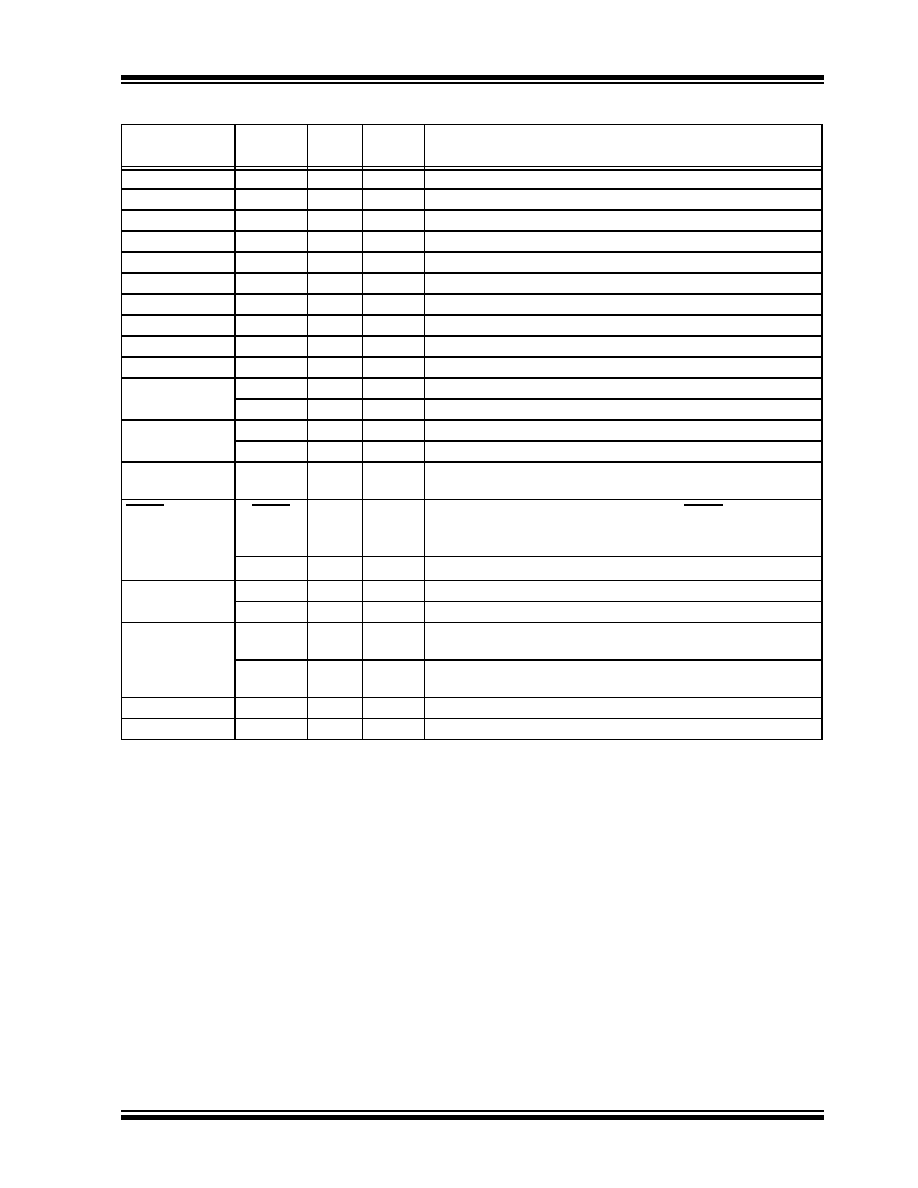
TABLE 2-1:
PIC16F54 PINOUT DESCRIPTION
Name
Function
Input
Type
Output
Type
Description
RA0
TTL
CMOS
Bidirectional I/O pin
RA1
TTL
CMOS
Bidirectional I/O pin
RA2
TTL
CMOS
Bidirectional I/O pin
RA3
TTL
CMOS
Bidirectional I/O pin
RB0
TTL
CMOS
Bidirectional I/O pin
RB1
TTL
CMOS
Bidirectional I/O pin
RB2
TTL
CMOS
Bidirectional I/O pin
RB3
TTL
CMOS
Bidirectional I/O pin
RB4
TTL
CMOS
Bidirectional I/O pin
RB5
TTL
CMOS
Bidirectional I/O pin
RB6/ICSPCLK
RB6
TTL
CMOS
Bidirectional I/O pin
ICSPCLK
ST
—
Serial Programming Clock
RB7/ICSPDAT
RB7
TTL
CMOS
Bidirectional I/O pin
ICSPDAT
ST
CMOS
Serial Programming I/O
T0CKI
ST
—
Clock input to Timer0. Must be tied to VSS or VDD, if not in use, to
reduce current consumption.
MCLR/VPP
MCLR
ST
—
Active-low Reset to device. Voltage on the MCLR/VPP pin must
not exceed VDD to avoid unintended entering of Programming
mode.
VPP
HV
—
Programming voltage input
OSC1/CLKIN
OSC1
XTAL
—
Oscillator crystal input
CLKIN
ST
—
External clock source input
OSC2/CLKOUT
OSC2
—
XTAL
Oscillator crystal output. Connects to crystal or resonator in
Crystal Oscillator mode.
CLKOUT
—
CMOS
In RC mode, OSC2 pin can output CLKOUT, which has 1/4 the
frequency of OSC1.
VDD
Power
—
Positive supply for logic and I/O pins
VSS
Power
—
Ground reference for logic and I/O pins
Legend: I
= input
I/O
= input/output
CMOS = CMOS output
O
= output
—
= Not Used
XTAL
= Crystal input/output
ST
= Schmitt Trigger input
TTL = TTL input
HV
= High Voltage
发布紧急采购,3分钟左右您将得到回复。
相关PDF资料
AT97SC3204-X1A50-1
CRYPTO TPM LPC 3.0-3.6V 28TSSOP
ATA6620N-TAQY
TXRX LIN BUS W/VREG SO-8
ATA6661-TAQJ 19
TXRX LIN 2.0 3.3V/5V 8SOIC
ATA6670-FFQW
IC TXRX LIN DUAL 14VDFN
ATAM893T-TKSYD
IC MCU FLASH 4K MTP 20SSOP
ATF1500ABV-15JI
IC CPLD 15NS LOW VOLT PLCC
ATF1500AL-20JI
IC CPLD 20NS LOW POW 44PLCC
ATF1502ASV-15JI44
IC CPLD EE HP 15NS 44-PLCC
相关代理商/技术参数
AT91SAM9XE-EK
功能描述:开发板和工具包 - ARM Eval Kit for SAM9XE Series
RoHS:否 制造商:Arduino 产品:Development Boards 工具用于评估:ATSAM3X8EA-AU 核心:ARM Cortex M3 接口类型:DAC, ICSP, JTAG, UART, USB 工作电源电压:3.3 V
AT91SAM-ICE
功能描述:仿真器/模拟器 JTAG emulator AT91 ARM7/ARM9 RoHS:否 制造商:Blackhawk 产品:System Trace Emulators 工具用于评估:C6000, C5000, C2000, OMAP, DAVINCI, SITARA, TMS470, TMS570, ARM 7/9, ARM Cortex A8/R4/M3 用于:XDS560v2
AT91SAMS64-AI
制造商:ATMEL 制造商全称:ATMEL Corporation 功能描述:AT91 ARM㈢ Thumb㈢-based Microcontrollers
AT91SC192192CT-USB
制造商:ATMEL 制造商全称:ATMEL Corporation 功能描述:32-bit Secure Microcontrollers
AT91SC25672RC
制造商:ATMEL 制造商全称:ATMEL Corporation 功能描述:32-bit Secure Microcontroller for Smart Cards
AT91SC321RC-MQC-AM2
功能描述:ARM微控制器 - MCU For Secure Trnsactns in Smart Crd/PC Apps RoHS:否 制造商:STMicroelectronics 核心:ARM Cortex M4F 处理器系列:STM32F373xx 数据总线宽度:32 bit 最大时钟频率:72 MHz 程序存储器大小:256 KB 数据 RAM 大小:32 KB 片上 ADC:Yes 工作电源电压:1.65 V to 3.6 V, 2 V to 3.6 V, 2.2 V to 3.6 V 工作温度范围:- 40 C to + 85 C 封装 / 箱体:LQFP-48 安装风格:SMD/SMT
AT91SC321RC-MQC-AM5
功能描述:ARM微控制器 - MCU For Secure Trnsactns in Smart Crd/PC Apps RoHS:否 制造商:STMicroelectronics 核心:ARM Cortex M4F 处理器系列:STM32F373xx 数据总线宽度:32 bit 最大时钟频率:72 MHz 程序存储器大小:256 KB 数据 RAM 大小:32 KB 片上 ADC:Yes 工作电源电压:1.65 V to 3.6 V, 2 V to 3.6 V, 2.2 V to 3.6 V 工作温度范围:- 40 C to + 85 C 封装 / 箱体:LQFP-48 安装风格:SMD/SMT
AT91SC321RC-MQC-AM7
功能描述:ARM微控制器 - MCU For Secure Trnsactns in Smart Crd/PC Apps RoHS:否 制造商:STMicroelectronics 核心:ARM Cortex M4F 处理器系列:STM32F373xx 数据总线宽度:32 bit 最大时钟频率:72 MHz 程序存储器大小:256 KB 数据 RAM 大小:32 KB 片上 ADC:Yes 工作电源电压:1.65 V to 3.6 V, 2 V to 3.6 V, 2.2 V to 3.6 V 工作温度范围:- 40 C to + 85 C 封装 / 箱体:LQFP-48 安装风格:SMD/SMT